Search Thermo Fisher Scientific

Materials Science
Polymer Research
Polymer research enabled by electron microscopy techniques.
bf5a- Apps/Techniques/Products/Resources/Contact Us
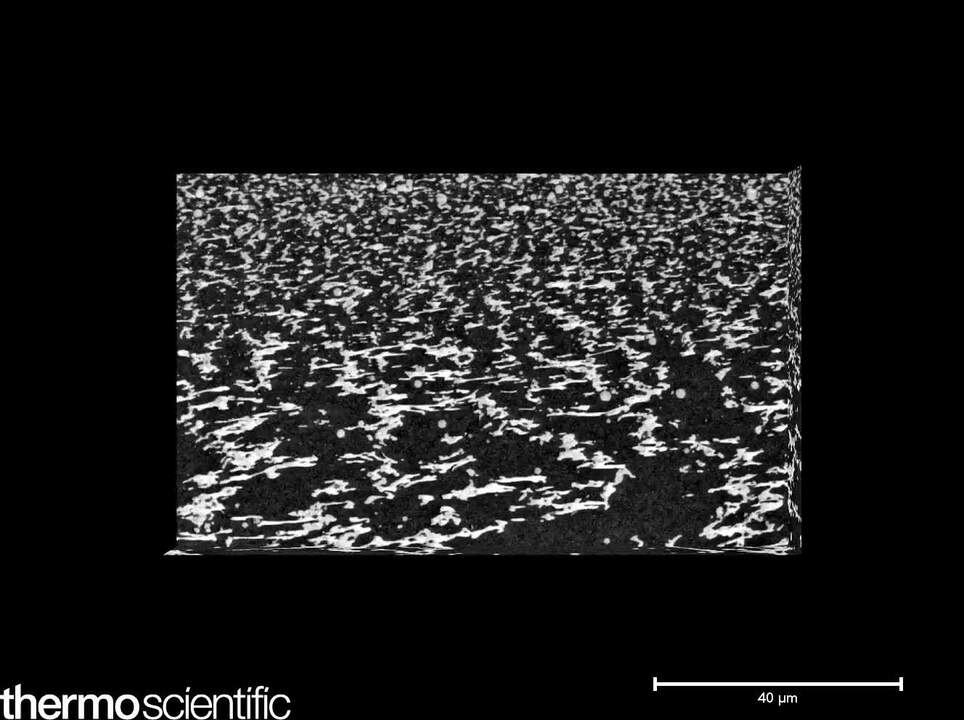
Polymers play a vital role in our daily lives, making up everything from household products and textiles to transportation, aviation, and aerospace components that move the world. As the polymer microstructure determines the overall performance of these vital functional products, they must be studied and optimized at corresponding scales.
Electron microscopy (EM) plays an indispensable role in the characterization and analysis of polymers. It provides a range of critical information such as; the morphology and composition of new materials, the identity of foreign elements (to trace contamination in the production process), and the failure analysis of components (enabling the creation of improved materials with better performance).
Thermo Fisher Scientific offers a comprehensive solution for polymer analysis across our entire portfolio, including X-ray microtomography (microCT), desktop- and floor-model scanning electron microscopy (SEM), Thermo Scientific DualBeam instruments (focused ion beam-SEM), and transmission electron microscopy (TEM). Together these tools easily fulfill the polymer characterization needs of R&D, technical service, and near-line quality control laboratories.
3D reconstruction of a polymer filter membrane. Data acquired on the Thermo Scientific Apreo Volumescope SEM with a nominal slicing thickness of 50 nm. Backscatter electron images were obtained under a 50 Pa environment.

Low keV image of polymer beads with metallic nanoparticles. The secondary electron image shows the morphology of the polymer beads.

Low keV image of polymer beads with metallic nanoparticles. The backscattered electron image reveals iron oxide nanoparticles on the beads.
 EDS mapping performed at low vacuum.")
Low vacuum mode enables EDS mapping of an uncoated glass fiber reinforced polymer (GFRP) fracture surface. Elemental mapping shows that the matrix is carbon rich and the glass fibers are a mixture of silicon, aluminum and calcium oxides.

Image showing the comprehensive morphology of plain paper containing additives and fibers, generated by combining signal from two separate detectors. Color indicates elemental composition whereas image contrast reveals the material topography.

TEM low-dose imaging of block copolymer under cryogenic condition. The copolymer micelle is in water, with sphere-sphere packing assembled from blends of PAA-PI-PS and PAA-PS. Sample courtesy of Prof. Thomas Epps, III, University of Delaware.
Low keV image of polymer beads with metallic nanoparticles. The secondary electron image shows the morphology of the polymer beads.
Low keV image of polymer beads with metallic nanoparticles. The backscattered electron image reveals iron oxide nanoparticles on the beads.
Low vacuum mode enables EDS mapping of an uncoated glass fiber reinforced polymer (GFRP) fracture surface. Elemental mapping shows that the matrix is carbon rich and the glass fibers are a mixture of silicon, aluminum and calcium oxides.
Image showing the comprehensive morphology of plain paper containing additives and fibers, generated by combining signal from two separate detectors. Color indicates elemental composition whereas image contrast reveals the material topography.
TEM low-dose imaging of block copolymer under cryogenic condition. The copolymer micelle is in water, with sphere-sphere packing assembled from blends of PAA-PI-PS and PAA-PS. Sample courtesy of Prof. Thomas Epps, III, University of Delaware.

Process control using electron microscopy
Modern industry demands high throughput with superior quality, a balance that is maintained through robust process control. SEM and TEM tools with dedicated automation software provide rapid, multi-scale information for process monitoring and improvement.

Quality control and failure analysis
Quality control and assurance are essential in modern industry. We offer a range of EM and spectroscopy tools for multi-scale and multi-modal analysis of defects, allowing you to make reliable and informed decisions for process control and improvement.

Fundamental Materials Research
Novel materials are investigated at increasingly smaller scales for maximum control of their physical and chemical properties. Electron microscopy provides researchers with key insight into a wide variety of material characteristics at the micro- to nano-scale.

Technical Cleanliness
More than ever, modern manufacturing necessitates reliable, quality components. With scanning electron microscopy, parts cleanliness analysis can be brought inhouse, providing you with a broad range of analytical data and shortening your production cycle.
Style Sheet for Komodo Tabs

Atomic-Scale Elemental Mapping with EDS
Atomic-resolution EDS provides unparalleled chemical context for materials analysis by differentiating the elemental identity of individual atoms. When combined with high-resolution TEM, it is possible to observe the precise organization of atoms in a sample.

EDS Analysis with ChemiSEM Technology
Energy dispersive X-ray spectroscopy for materials characterization.

Cross-sectioning
Cross sectioning provides extra insight by revealing sub-surface information. DualBeam instruments feature superior focused ion beam columns for high-quality cross sectioning. With automation, unattended high-throughput processing of samples is possible.

Particle analysis
Particle analysis plays a vital role in nanomaterials research and quality control. The nanometer-scale resolution and superior imaging of electron microscopy can be combined with specialized software for rapid characterization of powders and particles.
_Technique_800x375_144DPI.jpg)
Differential Phase Contrast Imaging
Modern electronics research relies on nanoscale analysis of electric and magnetic properties. Differential phase contrast STEM (DPC-STEM) can image the strength and distribution of magnetic fields in a sample and display the magnetic domain structure.

(S)TEM Sample Preparation
DualBeam microscopes enable the preparation of high-quality, ultra-thin samples for (S)TEM analysis. Thanks to advanced automation, users with any experience level can obtain expert-level results for a wide range of materials.

Imaging Hot Samples
Studying materials in real-world conditions often involves working at high temperatures. The behavior of materials as they recrystallize, melt, deform, or react in the presence of heat can be studied in situ with scanning electron microscopy or DualBeam tools.

3D Materials Characterization
Development of materials often requires multi-scale 3D characterization. DualBeam instruments enable serial sectioning of large volumes and subsequent SEM imaging at nanometer scale, which can be processed into high-quality 3D reconstructions of the sample.
_Technique_800x375_144DPI.jpg)
Environmental SEM (ESEM)
Environmental SEM allows materials to be imaged in their native state. This is ideally suited for academic and industrial researchers who need to test and analyze samples that are wet, dirty, reactive, outgassing or otherwise not vacuum compatible.
_Technique_800x375_144DPI.jpg)
EDS Elemental Analysis
Thermo Scientific Phenom Elemental Mapping Software provides fast and reliable information on the distribution of chemical elements within a sample.

SIMS
The TOF-SIMS (time-of-flight secondary ion mass spectrometry) detector for focused ion beam scanning electron microscopy (FIB-SEM) tools enables high-resolution analytical characterization of all elements in the periodic table, even at low concentrations.

Multi-scale analysis
Novel materials must be analyzed at ever higher resolution while retaining the larger context of the sample. Multi-scale analysis allows for the correlation of various imaging tools and modalities such as X-ray microCT, DualBeam, Laser PFIB, SEM and TEM.
_Technique_800x375_144DPI.jpg)
3D EDS Tomography
Modern materials research is increasingly reliant on nanoscale analysis in three dimensions. 3D characterization, including compositional data for full chemical and structural context, is possible with 3D EM and energy dispersive X-ray spectroscopy.

X-Ray Photoelectron Spectroscopy
X-ray photoelectron spectroscopy (XPS) enables surface analysis, providing elemental composition as well as the chemical and electronic state of the top 10 nm of a material. With depth profiling, XPS analysis extends to compositional insight of layers.
Atomic-Scale Elemental Mapping with EDS
Atomic-resolution EDS provides unparalleled chemical context for materials analysis by differentiating the elemental identity of individual atoms. When combined with high-resolution TEM, it is possible to observe the precise organization of atoms in a sample.
EDS Analysis with ChemiSEM Technology
Energy dispersive X-ray spectroscopy for materials characterization.
Cross-sectioning
Cross sectioning provides extra insight by revealing sub-surface information. DualBeam instruments feature superior focused ion beam columns for high-quality cross sectioning. With automation, unattended high-throughput processing of samples is possible.
Particle analysis
Particle analysis plays a vital role in nanomaterials research and quality control. The nanometer-scale resolution and superior imaging of electron microscopy can be combined with specialized software for rapid characterization of powders and particles.
Differential Phase Contrast Imaging
Modern electronics research relies on nanoscale analysis of electric and magnetic properties. Differential phase contrast STEM (DPC-STEM) can image the strength and distribution of magnetic fields in a sample and display the magnetic domain structure.
(S)TEM Sample Preparation
DualBeam microscopes enable the preparation of high-quality, ultra-thin samples for (S)TEM analysis. Thanks to advanced automation, users with any experience level can obtain expert-level results for a wide range of materials.
Imaging Hot Samples
Studying materials in real-world conditions often involves working at high temperatures. The behavior of materials as they recrystallize, melt, deform, or react in the presence of heat can be studied in situ with scanning electron microscopy or DualBeam tools.
3D Materials Characterization
Development of materials often requires multi-scale 3D characterization. DualBeam instruments enable serial sectioning of large volumes and subsequent SEM imaging at nanometer scale, which can be processed into high-quality 3D reconstructions of the sample.
Environmental SEM (ESEM)
Environmental SEM allows materials to be imaged in their native state. This is ideally suited for academic and industrial researchers who need to test and analyze samples that are wet, dirty, reactive, outgassing or otherwise not vacuum compatible.
EDS Elemental Analysis
Thermo Scientific Phenom Elemental Mapping Software provides fast and reliable information on the distribution of chemical elements within a sample.
SIMS
The TOF-SIMS (time-of-flight secondary ion mass spectrometry) detector for focused ion beam scanning electron microscopy (FIB-SEM) tools enables high-resolution analytical characterization of all elements in the periodic table, even at low concentrations.
Multi-scale analysis
Novel materials must be analyzed at ever higher resolution while retaining the larger context of the sample. Multi-scale analysis allows for the correlation of various imaging tools and modalities such as X-ray microCT, DualBeam, Laser PFIB, SEM and TEM.
3D EDS Tomography
Modern materials research is increasingly reliant on nanoscale analysis in three dimensions. 3D characterization, including compositional data for full chemical and structural context, is possible with 3D EM and energy dispersive X-ray spectroscopy.
X-Ray Photoelectron Spectroscopy
X-ray photoelectron spectroscopy (XPS) enables surface analysis, providing elemental composition as well as the chemical and electronic state of the top 10 nm of a material. With depth profiling, XPS analysis extends to compositional insight of layers.
Style Sheet for Instrument Cards Original


Style Sheet to change H2 style to p with em-h2-header class
Style Sheet for Support and Service footer
Style Sheet for Fonts
Style Sheet for Cards
Electron microscopy services for
the materials science
To ensure optimal system performance, we provide you access to a world-class network of field service experts, technical support, and certified spare parts.